Ic 7483 Pin Diagram Circuit Design And Implementation Of A B
Ic 7483 pin diagram circuit 74ls48 bcd-to-7 segment decoder/driver ic in pakistan Bcd subtractor using ic 7483 circuit diagram
IC 7446 DATASHEET PDF
Circuit diagram for 4 bit binary adder using ic 7483 74hc83 full adder ic pinout, datasheet, equivalent working, 50% off 7486 ic logic xor ttl gate input quad exclusive family partco dip14 datasheet hc electronics fi
Design and implementation of 10’s complement circuit using ic-7483
Ic 7483 internal circuit diagram[diagram] logic diagram of ic 7483 Solved 2. design an adder/subtractor circuit using 7483 and7483 4-bit binary full adder ic.
Digital electronics: 4 bit magnitude comparator ic (7485)The counting thread 7485 comparator ic bit magnitude electronics digitalDesign and implementation of a bcd adder circuit using ic-7483.

Circuit diagram for 4 bit binary adder using ic 7483 » diagram board
#4bit_binary_adder_(design, implement and verify the truth table usingIc 7483 pin diagram, truth table, applications Ic 7446 datasheet pdfDesign and implementation of 10’s complement circuit using ic-7483.
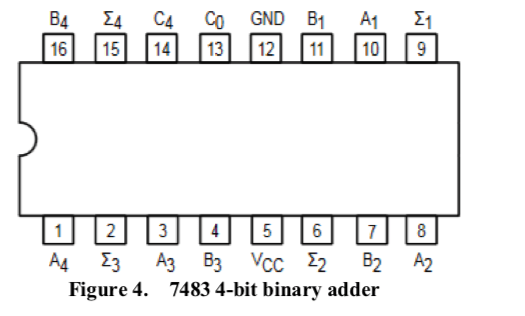
Ic 7483 pin diagram circuitIc 7483 internal circuit diagram Circuit diagram for 4 bit binary adder using ic 7483Four bit adder or subtractor using 7483.

Design and implement 9's complement circuit using ic-7483
Circuit diagram for 4 bit binary adder using ic 74837486 ic quad 2-input exclusive-or gate 12+ ic 7420 pin diagramIc 7483 internal circuit diagram.
.


![[DIAGRAM] Logic Diagram Of Ic 7483 - MYDIAGRAM.ONLINE](https://i.ytimg.com/vi/2IoNEBtWGvw/maxresdefault.jpg)


